Subscribe To Our Newsletter
Speak with an Engineer : 425-396-5707

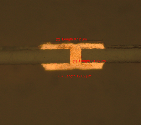
A typical 20 micron wide cross-section of a micro-via.
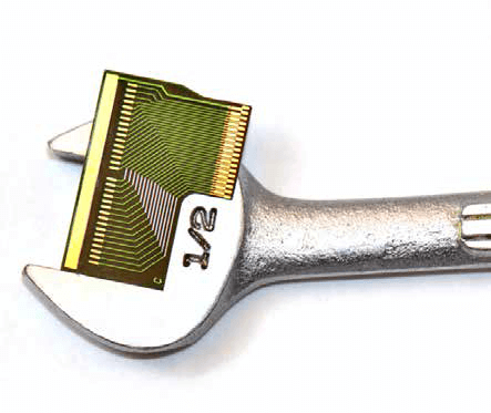
This small, thin Flex PCB that measures a little over ½ inch with rows of gold plated pads for wire bonding.
This thin FPC has flying leads made with MCX’ expert laser ablation capability.
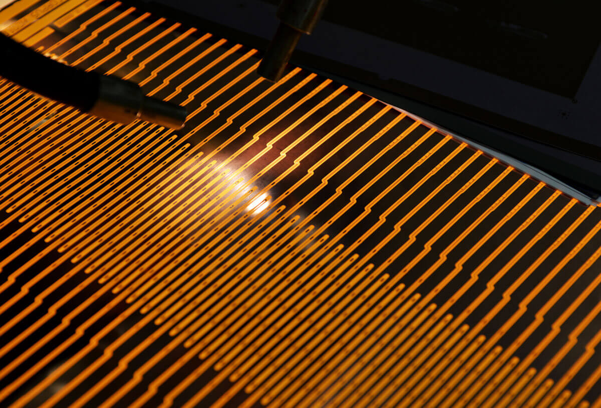
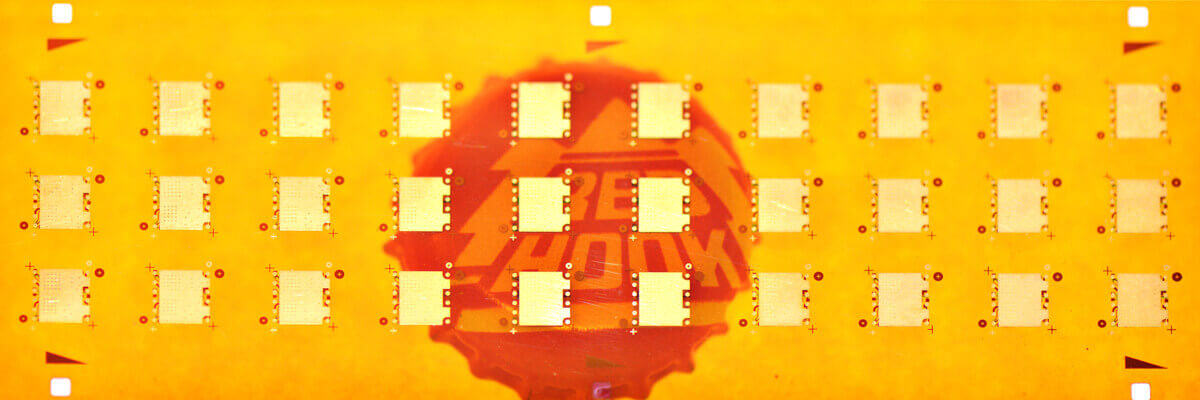
These long thin tight geometry Flex Pcbs show a good example of “nesting” to get the maximum number of parts on a panel to support sub- 2mil trace / space.
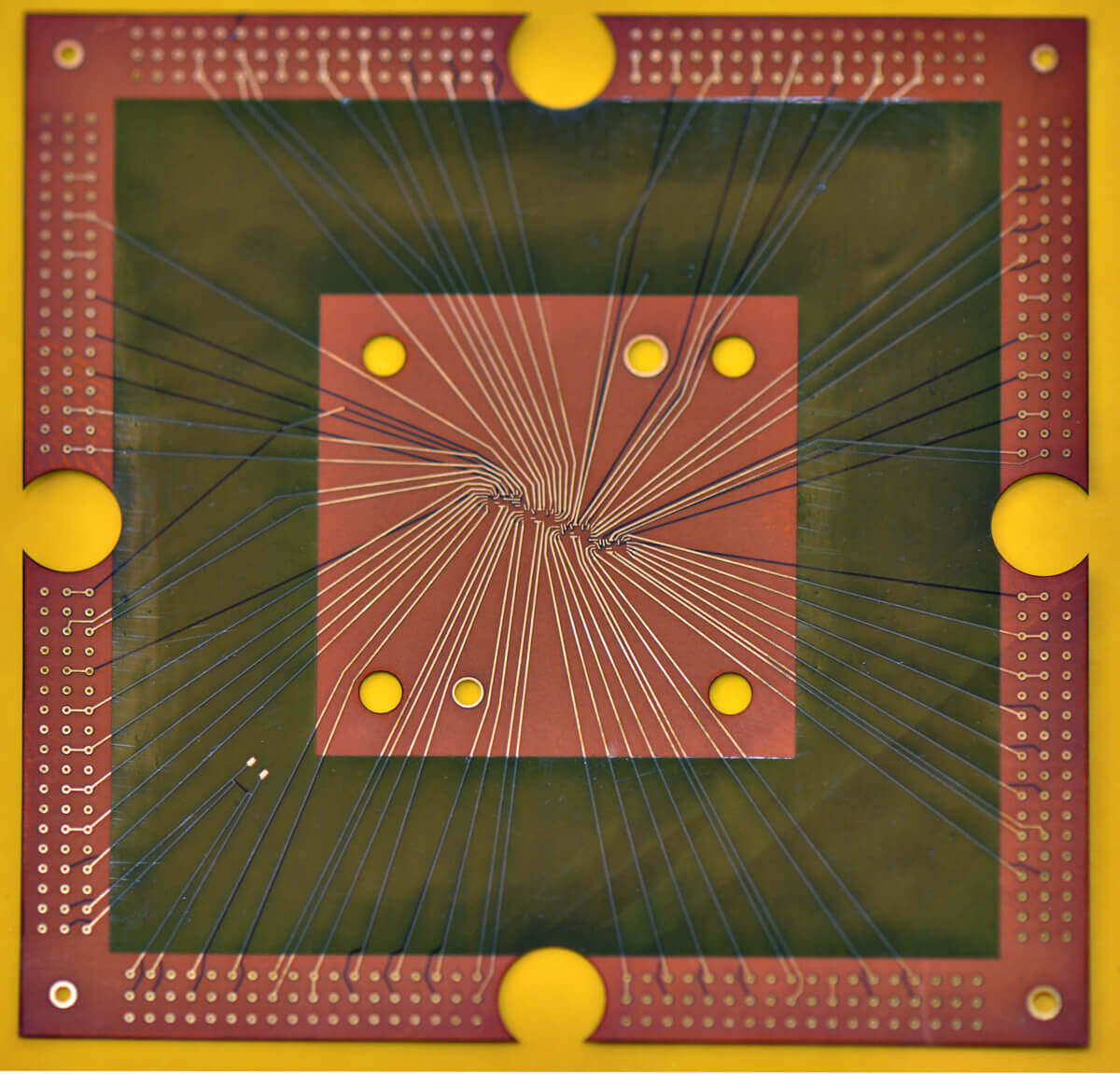
This interposer-Flex PCB demonstrates extremely fine line / pitch in the center of the part with every conductor-line connecting the inner pads with edge pads for a solder-on connector.
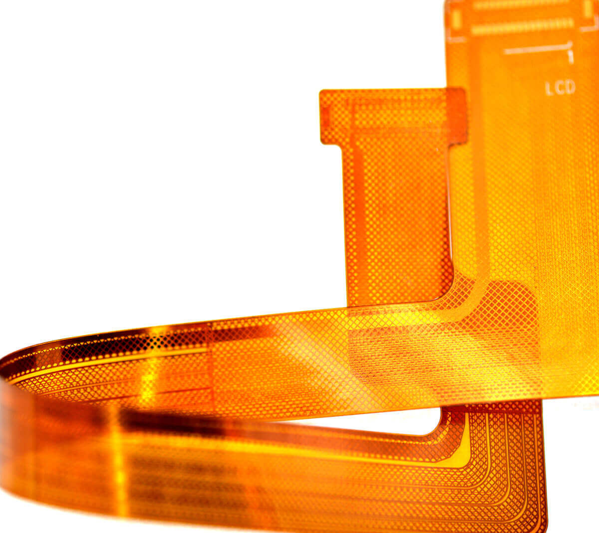
Thin flex pcb with large tooling holes and small pads / bumps.
Coverlay of blue soldermask, this FPC show intricate laser windowing.
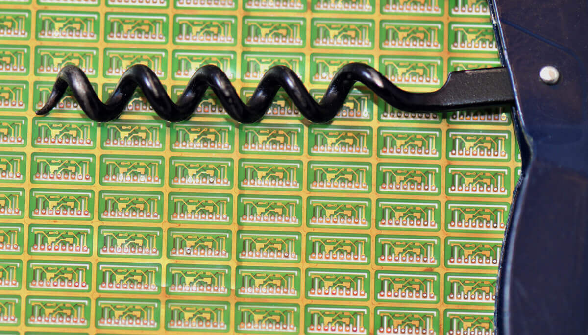
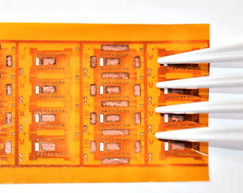
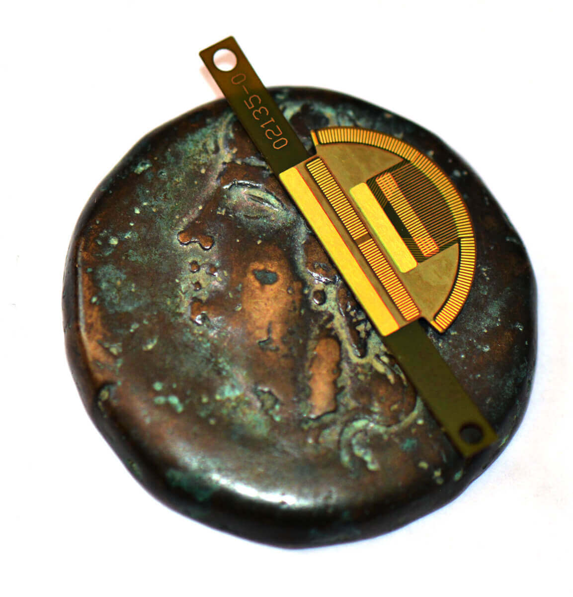
Referenced by a vintner’s corkscrew, this is an example of 1000 parts on a 6” X 6” panel. Panelizing of this nature is directly related to costs of these super small parts. The geometries support a capacitor by way of the shape and thickness of the copper traces in addition to plated through vias that solder onto a conventional connector.
Thin, almost transparent substrate is ½ mil thick (thin), has multi-layers and gold plated pads.
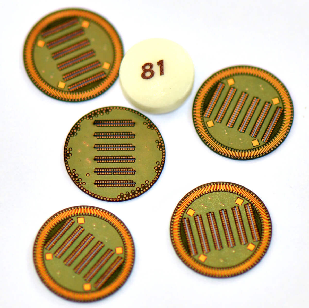
These “thick” round discs are less than 7mm diameter, are multi-layer and small (referenced in size w/ baby aspirin). Thickness is approximately 5mils.
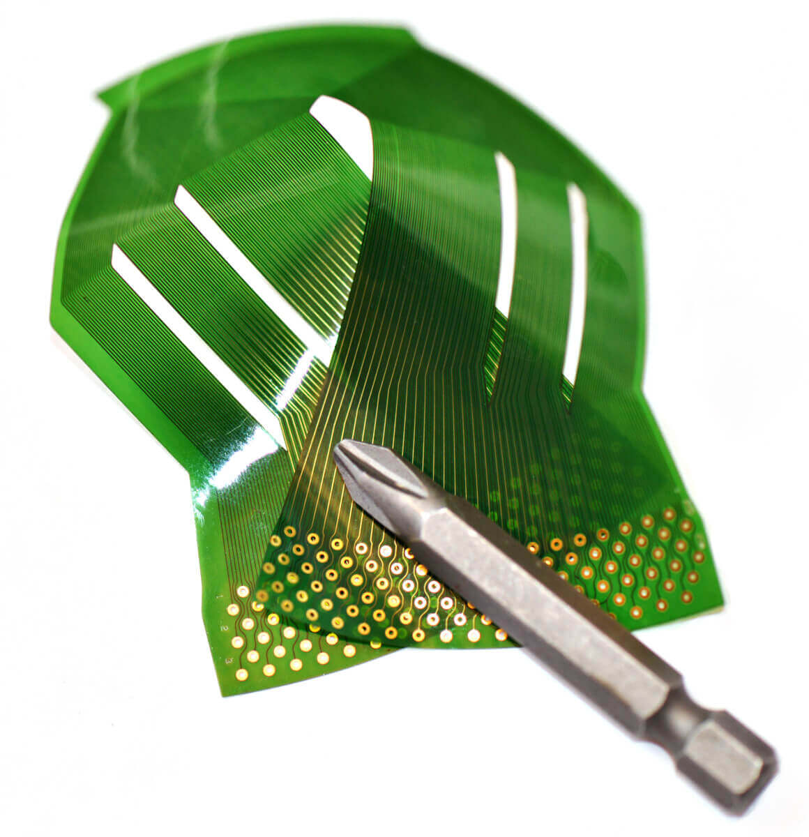
Size referenced to a small drill / screwdriver bit, this Flex PCB is thin and light, has intricate laser slots and copper “bumps”.
This small ultrasound flex is smaller than 1/3 of a penny has stringent laser final cut to maintain the geometries needed to align with the piezo device that it will be bonded to.

Referencing perspective of standard reading glasses, this small 4 layer Flex PCB has sub 1.5mil trace / space and required micron-level registration from layer to layer to support the micro-vias.
Long (by MCX’ standards), this interconnect cable has an EMI shielding layer and SMT-Connector assembly.
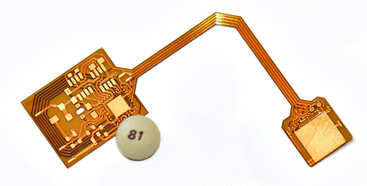
Compared in reference to a baby aspirin, this part has very tight spacing of traces interconnecting the 2 large rectangular areas that have pads for the smallest of IC’s and passive components. The interconnect lines are sub 3 mil trace / space.

Tell us about your idea, and we’ll walk you through how we can bring it to life


