Ensuring Excellence in Flex PCB Manufacturing: Quality Assurance at MicroConnex

Excellence in Flex PCB Manufacturing: Quality Assurance at MicroConnex

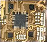
At MicroConnex, the quality of our flexible printed circuit boards (FPCBs) is paramount. To ensure that each PCB meets our high standards, we employ a comprehensive quality assurance process that integrates cutting-edge technology and meticulous testing procedures.

Automated Testing with Flying Probe Machine

A cornerstone of our quality assurance is the use of an automated flying probe machine. This advanced equipment is crucial for testing the continuity of circuits efficiently and accurately. By employing a non-contact method that rapidly tests multiple points on a circuit board, the flying probe machine can identify any potential issues with electrical connectivity without the need for a physical test fixture. This process not only speeds up the testing phase but also reduces the risk of damaging the delicate circuits on FPCBs.

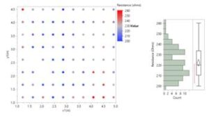
Automated Dimensional Verification

To complement our electrical testing, we utilize automated dimensional verification systems. These systems provide high-precision inspection capabilities that ensure all physical dimensions of our PCBs adhere strictly to design specifications. By catching even the smallest deviations, we can guarantee that every batch of FPCBs meets both our standards and the exacting requirements of our clients.

Laser Removal of Shorts Detected During Inspection

If any shorts are detected during the inspection process, our facility is equipped with state-of-the-art laser technology to address these defects promptly. The precision of laser removal allows us to correct faults with minimal impact on the surrounding circuitry, thereby maintaining the integrity and functionality of the entire board.

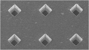
Optical CMM with Exceptional Accuracy

Further enhancing our quality assurance capabilities is the optical Coordinate Measuring Machine (CMM). This sophisticated equipment boasts linear accuracy up to 5 microns and Z-axis accuracy up to 3 microns. Such high-resolution measurements are critical in ensuring that every aspect of our FPCBs is produced with absolute precision, from the placement of components to the alignment of layers.

Commitment to Quality

The integration of these advanced testing and correction technologies underscores MicroConnex’s commitment to quality. By continually investing in the latest quality assurance technologies, we not only adhere to industry standards but often exceed them, ensuring that our clients receive products that are reliable, durable, and precise.

Conclusion

Quality assurance at MicroConnex is not just a process; it’s a cornerstone of our manufacturing philosophy. From automated flying probe testing to precise dimensional verification and laser correction, every step in our production is designed to ensure that the FPCBs we produce stand up to the demands of the most critical applications. Our approach is proactive, meticulous, and always evolving, reflecting our commitment to excellence and customer satisfaction.

By choosing MicroConnex for your flex PCB needs, you are partnering with a company that places quality at the forefront of its operations, ensuring that every product not only meets but exceeds expectations. Whether for medical devices, aerospace components, or consumer electronics, our PCBs are built to perform flawlessly in any application.


Enhancing Flex PCBs with Advanced Electroplating Techniques

Enhancing Flex PCBs with Advanced Electroplating Techniques

Electroplating is a critical process in the manufacturing of flexible printed circuit boards (FPCBs), significantly enhancing their conductivity, durability, and overall performance. At MicroConnex, we offer a variety of advanced electroplating options to meet diverse application needs, including ENIG, NI/Au, ENPIG, Immersion Sn, and Immersion Ag.

ENIG (Electroless Nickel Immersion Gold): ENIG is widely favored for its excellent surface planarity and long shelf life. This process involves a layer of nickel covered by a thin layer of gold, providing a robust, solderable surface. The gold layer protects the nickel from oxidation, ensuring reliable performance during soldering and component attachment. This combination results in a surface finish that is highly durable and reliable, making it an excellent choice for high-performance applications.

NI/Au (Nickel/Gold): This method, commonly used in high-reliability applications, involves electroplating a nickel layer followed by a gold layer. NI/Au plating offers exceptional corrosion resistance and excellent electrical conductivity, making it ideal for contacts and connectors in flex PCBs. The robustness of this finish is particularly beneficial in harsh environments, where maintaining electrical connectivity and preventing corrosion are paramount.

ENPIG (Electroless Nickel Palladium Immersion Gold): ENPIG combines nickel, palladium, and gold layers, offering enhanced protection against oxidation and corrosion. The palladium layer acts as a barrier, preventing gold from diffusing into the nickel layer, thus maintaining the integrity of the solder joints and ensuring high durability. This makes ENPIG particularly suitable for applications requiring frequent soldering and desoldering, as it maintains excellent joint integrity over multiple cycles.

Immersion Sn (Tin): Immersion Tin is a cost-effective solution that provides a flat, solderable surface ideal for fine-pitch components. It offers good solderability and is an excellent choice for lead-free assembly processes, ensuring reliable performance without the environmental concerns associated with lead-based finishes. The uniform and smooth finish of Immersion Tin is beneficial for high-density interconnects (HDI), where precise soldering is essential.

Immersion Ag (Silver): Immersion Silver is known for its excellent electrical conductivity and cost-effectiveness. This finish provides a smooth, solderable surface, making it suitable for high-frequency applications where signal integrity is crucial. Additionally, it offers good resistance to thermal cycling, ensuring longevity in demanding environments. Immersion Silver’s excellent conductivity and planarity make it ideal for RF applications, where signal loss must be minimized.

Why Choose MicroConnex as Your Flex PCB Manufacturing Partner?

At MicroConnex, we understand the diverse requirements of modern flex PCB applications. Our commitment to delivering high-quality, reliable, and customized solutions sets us apart. We offer a range of advanced surface finish options, including ENIG, NI/Au, ENPIG, Immersion Sn, and Immersion Ag, to ensure your flex PCBs meet the highest standards of performance and reliability. Our expertise in precision manufacturing, combined with our comprehensive electroplating capabilities, makes us the ideal partner for your flex PCB production needs.

We are dedicated to innovation and excellence, ensuring that our manufacturing processes incorporate the latest advancements in technology. Our state-of-the-art facilities and skilled workforce enable us to deliver products that meet the most stringent industry standards. By partnering with MicroConnex, you gain access to a wealth of knowledge and experience, ensuring that your projects are completed efficiently and to the highest quality.

Partner with MicroConnex

With our expertise in precision manufacturing and advanced electroplating techniques, MicroConnex is your ideal partner for flex PCB production. We are committed to delivering high-quality, reliable, and customized solutions that meet your specific requirements. Our focus on innovation and quality assurance ensures that every product we deliver performs reliably in its intended application. Contact us today to learn more about how we can help you achieve the best results for your flex PCB projects. Whether you need the robustness of ENIG, the high conductivity of NI/Au, the durability of ENPIG, or the cost-effectiveness of Immersion Sn and Ag, MicroConnex has the right solution for your needs.


Precision in Flex PCB Manufacturing: Laser Direct Imaging (LDI)

Free circuit board circuits control center illustration

Precision in Flex PCB Manufacturing: Laser Direct Imaging (LDI)

In the realm of flexible printed circuit boards (FPCBs), achieving high precision and flexibility is crucial. One standout technology in this domain is Laser Direct Imaging (LDI). Unlike traditional photolithography, LDI offers unique advantages that can significantly enhance the manufacturing process of flex PCBs.

Understanding Laser Direct Imaging (LDI)

Laser Direct Imaging (LDI) is a process that uses focused laser beams to directly write circuit patterns onto a photoresist-coated substrate. This technique eliminates the need for photomasks, which are essential in traditional photolithography. The direct nature of LDI not only speeds up the manufacturing process but also offers greater flexibility in design adjustments.

Advantages for Flex PCBs

  1. Flexibility and Speed: LDI allows for rapid design changes and prototyping since it bypasses the need for creating and modifying masks. This is particularly beneficial for custom designs and small production runs.
  2. High Precision: While photolithography is known for its high resolution, LDI provides excellent precision suitable for most flex PCB applications. It can achieve fine features and complex patterns, crucial for modern electronic devices.
  3. Cost-Effectiveness: By eliminating the need for masks, LDI reduces production costs, especially in the early stages of product development. This makes it an attractive option for companies looking to optimize their manufacturing budgets.
  4. Improved Throughput: LDI can significantly enhance throughput by streamlining the imaging process. This leads to shorter production cycles and faster time-to-market for new products.

Applications and Benefits

Laser Direct Imaging is particularly valuable in industries where rapid prototyping and customization are essential. For example:

  • Medical Devices: Flex PCBs with intricate and precise patterns are critical for the reliability and functionality of medical equipment.
  • Aerospace: The ability to quickly iterate on designs ensures that aerospace components meet stringent performance and reliability standards.
  • Consumer Electronics: As devices become smaller and more complex, the precision and flexibility offered by LDI are indispensable.

Why Consider LDI for Flex PCBs?

Given its speed, flexibility, and cost-effectiveness, LDI is a powerful tool for flex PCB manufacturing. It provides manufacturers with the ability to quickly respond to design changes, reduce production costs, and maintain high precision. These advantages make LDI an ideal choice for companies looking to stay competitive in the fast-paced electronics industry.

Partnering for Success

At MicroConnex, we leverage advanced LDI technology to deliver high-quality flex PCBs tailored to your specific needs. Whether you’re developing cutting-edge medical devices or sophisticated aerospace systems, our expertise in precision manufacturing ensures that your projects meet the highest standards of performance and reliability.

By incorporating Laser Direct Imaging into your manufacturing process, you can achieve greater flexibility, precision, and efficiency. Let MicroConnex be your partner in advancing your flex PCB capabilities.


Precision Meets Flexibility: Laser Micro-Machining for Flex PCB Manufacturing

Precision Meets Flexibility: Laser Micro-Machining for Flex PCB Manufacturing

As the demand for smaller, more versatile electronic devices grows, the need for precise and intricate manufacturing processes has become paramount. One such technology that is redefining the landscape of flexible printed circuit board (FPCB) manufacturing is laser micro-machining. At MicroConnex, we leverage this cutting-edge technology to push the boundaries of what’s possible in flex PCB design and production.

Understanding Laser Micro-Machining for Flex PCBs

Laser micro-machining involves using focused laser beams to cut, drill, or engrave materials with exceptional precision. This process is particularly well-suited for flexible printed circuit boards (flex PCBs), where creating fine features and complex patterns is essential. Unlike traditional mechanical methods, laser micro-machining is a non-contact process, which means it doesn’t exert physical stress on the flex PCB material, preserving its integrity and enhancing the overall quality of the final product.

Laser Micro-Machining in Flex PCB Manufacturing:

  1. High Precision and Resolution: Laser micro-machining offers unparalleled precision, enabling the creation of features as small as10 microns on flex PCBs. To put this into perspective, a human hair is typically about 70 microns in diameter. This means that the features we can create with laser micro-machining are roughly one-seventh the width of a human hair. Such an ultra-fine resolution is crucial for the miniaturization trends in electronics, where densely packed components and fine traces are standard. Achieving such tiny feature sizes ensures that even the most complex and intricate designs on flex PCBs can be executed flawlessly. Whether it’s cutting intricate patterns or drilling micro-vias, lasers provide the accuracy needed to meet tight tolerances and ensure the functionality of advanced flex PCBs.
  2. Versatility with Various Flex PCB Materials: Flex PCBs are often composed of multiple layers of different materials, including polyimide films, copper foils, and adhesives. Laser micro-machining is highly adaptable and can handle these diverse flex PCB substrates efficiently. Its ability to process a wide range of materials without altering their fundamental properties makes it ideal for the complex stack-ups typical in flex PCB designs.
  3. Enhanced Design Flexibility for Flex PCBs: Withlaser micro-machining, designers are no longer constrained by the limitations of conventional tooling. The precision of lasers allows for greater creativity and complexity in flex PCB design, enabling more innovative and functional electronic products. From curved traces to intricate cutouts, lasers can execute designs on flex PCBs that were previously difficult or impossible to achieve with traditional methods.
  4. Improved Manufacturing Efficiency for Flex PCBs: The speed and automation capabilities of laser micro-machining significantly enhance manufacturing efficiency for flex PCBs. The process can be easily integrated into automated production lines, reducing cycle times and increasing throughput. Additionally, the precise nature of laser machining minimizes material wastage on flex PCBs, contributing to more cost-effective production.
  5. Non-Contact Process Ideal for Flex PCBs:One of the most significant benefits of laser micro-machining is its non-contact nature. This aspect is particularly important for delicate flex PCBs, which can be susceptible to damage from mechanical processes. By eliminating physical contact, lasers preserve the material’s properties and reduce the risk of defects, leading to higher quality and more reliable flex PCB products.

MicroConnex: Your Partner in Advanced Flex PCB Solutions

At MicroConnex, we harness the power of laser micro-machining to deliver unparalleled precision and flexibility in flex PCB manufacturing. Our advanced laser systems are capable of performing a wide range of operations on flex PCBs, from fine cutting and drilling to precise patterning and engraving. Coupled with our experienced engineering team, we provide custom solutions that meet the unique needs of our clients in the flex PCB industry.

Collaborative Approach to Flex PCB Design: We work closely with our clients to understand their specific requirements and challenges in flex PCB manufacturing. Our collaborative approach ensures that we provide tailored solutions that not only meet but exceed expectations. Whether you’re developing next-generation medical devices, aerospace components, or consumer electronics, we’re here to help bring your flex PCB vision to life.

Commitment to Quality in Flex PCB Production: Quality is at the core of everything we do. Our laser micro-machining processes for flex PCBs are meticulously controlled and monitored to ensure each project meets the highest standards. This commitment to excellence ensures that our flex circuits perform reliably in the most demanding applications.

Conclusion

Laser micro-machining is transforming the flex PCB manufacturing industry by providing the precision and flexibility needed for today’s advanced electronic designs. The ability to create features as fine as 10 microns—about one-seventh the width of a human hair—opens up new possibilities for the miniaturization and complexity of circuits on flex PCBs. At MicroConnex, we utilize this advanced technology to offer innovative solutions that empower our clients to achieve their goals. Contact us today to explore how laser micro-machining can enhance your flex PCB projects and take your products to the next level.

Ready to take advantage of the precision and versatility of laser micro-machining for your flex PCB designs? Reach out to MicroConnex to discuss your project and discover how we can help you achieve unprecedented levels of performance and reliability in your flex PCB applications.