The Role of XRF in the Inspection of Flexible Circuits
The Role of XRF in the Inspection of Flexible Circuits
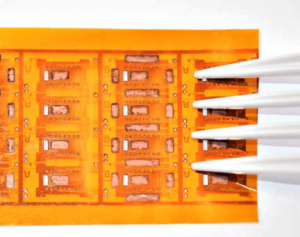
Flexible circuits (flex circuits) are increasingly used in various industries due to their lightweight, compact, and versatile nature. Whether in medical devices, aerospace, automotive systems, or consumer electronics, flex circuits allow for high-density connections and complex designs that are crucial for advanced technological solutions. However, ensuring the quality, reliability, and performance of these circuits requires precise inspection methods. One of the most powerful tools for this purpose is X-ray fluorescence (XRF) spectroscopy.
XRF is a non-destructive analytical technique that uses the interaction of X-rays with materials to determine their elemental composition. In the context of flex circuits, XRF is highly valuable for inspecting solder joints, plating thickness, material composition, and contamination, among other parameters.
Why Inspect Flex Circuits?
Flexible circuits are subject to complex stresses during manufacturing, assembly, and use. Due to their thin and bendable nature, flex circuits are prone to failure if not properly inspected for material consistency, plating uniformity, and contamination. Such failures can result in signal loss, mechanical breakdown, or complete device failure. Additionally, the miniaturization of electronics requires tighter tolerances, making the accuracy and precision of inspection methods more important than ever.
XRF helps manufacturers and engineers overcome these challenges by providing fast, accurate, and non-destructive testing at various stages of production and post-assembly.
Key Applications of XRF in Flex Circuit Inspection
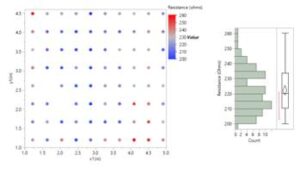
- Plating Thickness Measurement
Flex circuits often require precise plating layers on their copper traces, such as gold or nickel, to improve conductivity and prevent oxidation. XRF is widely used to measure the thickness of these plating layers to ensure they meet design specifications. For example, in fine-pitch flexible circuits, where conductive paths are tightly packed, slight variations in plating thickness can lead to significant performance issues. XRF provides accurate data on plating thickness, ensuring that the final product adheres to the required standards. - Elemental Composition of Solder Joints
Solder joints in flex circuits play a critical role in ensuring electrical continuity and mechanical stability. The composition of solder must meet precise specifications, typically requiring a specific ratio of tin (Sn), lead (Pb), or other metals such as silver (Ag) or copper (Cu). XRF can quickly identify the elemental composition of these solder joints, verifying that the materials used are compliant with design and regulatory standards. This is especially important for lead-free solder, where RoHS (Restriction of Hazardous Substances) compliance is required. - Contamination Detection
Contamination can seriously degrade the performance of flex circuits, particularly in high-reliability applications such as aerospace or medical devices. XRF allows for the detection of unwanted elements, such as residue from manufacturing processes or impurities introduced during assembly. Since XRF can detect trace levels of contamination down to parts-per-million (ppm), it is an invaluable tool for ensuring the purity and integrity of materials used in flex circuits. - Failure Analysis
In cases of flex circuit failure, XRF is a key tool for determining root causes. By analyzing the elemental composition of faulty areas, engineers can identify issues such as material degradation, corrosion, or incorrect solder compositions. This data is crucial for improving design processes and preventing future failures, especially in critical applications like medical devices or military systems.
Benefits of Using XRF in Flex Circuit Inspection
- Non-Destructive Testing: One of the main advantages of XRF is that it does not alter or damage the sample being analyzed. This is critical in high-value, delicate flex circuits, where minimizing scrap and rework is essential.
- Speed and Efficiency: XRF provides rapid results, allowing for real-time inspection during various stages of manufacturing. This helps manufacturers reduce bottlenecks and maintain high throughput without compromising quality.
- High Sensitivity: XRF instruments are capable of detecting trace elements at very low concentrations, which is important for ensuring that all materials used in flex circuits are pure and consistent.
- Versatility: XRF can be used to inspect a wide variety of materials, from metals to plastics, making it ideal for complex, multi-layered flex circuits.
Conclusion
As the demand for flexible circuits continues to grow in industries like electronics, medical devices, and aerospace, the need for precise, non-destructive inspection methods has never been greater. XRF stands out as a powerful tool for ensuring the quality, reliability, and compliance of flex circuits. From measuring plating thickness to analyzing solder joints and detecting contamination, XRF provides critical insights that help manufacturers produce high-performance, defect-free flex circuits. By leveraging XRF, companies can enhance their quality control processes, reduce costs associated with rework and failures, and deliver reliable products that meet the highest standards.
At MicroConnex, we specialize in advanced flex circuit manufacturing and inspection, utilizing XRF and other cutting-edge metrology tools to ensure top-notch quality. If you’re looking to learn more about XRF capabilities or other inspection technologies, or if you’re interested in partnering with our experienced applications engineers to develop your next flexible printed circuit (FPC) design, reach out to us today. Our team is ready to support you in bringing your innovative designs to life with precision and reliability. Contact us now to start a conversation and explore how we can help with your project.