Precision Meets Flexibility: Laser Micro-Machining for Flex PCB Manufacturing

Precision Meets Flexibility: Laser Micro-Machining for Flex PCB Manufacturing

As the demand for smaller, more versatile electronic devices grows, the need for precise and intricate manufacturing processes has become paramount. One such technology that is redefining the landscape of flexible printed circuit board (FPCB) manufacturing is laser micro-machining. At MicroConnex, we leverage this cutting-edge technology to push the boundaries of what’s possible in flex PCB design and production.

Understanding Laser Micro-Machining for Flex PCBs

Laser micro-machining involves using focused laser beams to cut, drill, or engrave materials with exceptional precision. This process is particularly well-suited for flexible printed circuit boards (flex PCBs), where creating fine features and complex patterns is essential. Unlike traditional mechanical methods, laser micro-machining is a non-contact process, which means it doesn’t exert physical stress on the flex PCB material, preserving its integrity and enhancing the overall quality of the final product.
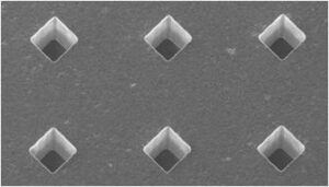
Laser Micro-Machining in Flex PCB Manufacturing:

  1. High Precision and Resolution: Laser micro-machining offers unparalleled precision, enabling the creation of features as small as10 microns on flex PCBs. To put this into perspective, a human hair is typically about 70 microns in diameter. This means that the features we can create with laser micro-machining are roughly one-seventh the width of a human hair. Such an ultra-fine resolution is crucial for the miniaturization trends in electronics, where densely packed components and fine traces are standard. Achieving such tiny feature sizes ensures that even the most complex and intricate designs on flex PCBs can be executed flawlessly. Whether it’s cutting intricate patterns or drilling micro-vias, lasers provide the accuracy needed to meet tight tolerances and ensure the functionality of advanced flex PCBs.
  2. Versatility with Various Flex PCB Materials: Flex PCBs are often composed of multiple layers of different materials, including polyimide films, copper foils, and adhesives. Laser micro-machining is highly adaptable and can handle these diverse flex PCB substrates efficiently. Its ability to process a wide range of materials without altering their fundamental properties makes it ideal for the complex stack-ups typical in flex PCB designs.
  3. Enhanced Design Flexibility for Flex PCBs: Withlaser micro-machining, designers are no longer constrained by the limitations of conventional tooling. The precision of lasers allows for greater creativity and complexity in flex PCB design, enabling more innovative and functional electronic products. From curved traces to intricate cutouts, lasers can execute designs on flex PCBs that were previously difficult or impossible to achieve with traditional methods.
  4. Improved Manufacturing Efficiency for Flex PCBs: The speed and automation capabilities of laser micro-machining significantly enhance manufacturing efficiency for flex PCBs. The process can be easily integrated into automated production lines, reducing cycle times and increasing throughput. Additionally, the precise nature of laser machining minimizes material wastage on flex PCBs, contributing to more cost-effective production.
  5. Non-Contact Process Ideal for Flex PCBs:One of the most significant benefits of laser micro-machining is its non-contact nature. This aspect is particularly important for delicate flex PCBs, which can be susceptible to damage from mechanical processes. By eliminating physical contact, lasers preserve the material’s properties and reduce the risk of defects, leading to higher quality and more reliable flex PCB products.

MicroConnex: Your Partner in Advanced Flex PCB Solutions

At MicroConnex, we harness the power of laser micro-machining to deliver unparalleled precision and flexibility in flex PCB manufacturing. Our advanced laser systems are capable of performing a wide range of operations on flex PCBs, from fine cutting and drilling to precise patterning and engraving. Coupled with our experienced engineering team, we provide custom solutions that meet the unique needs of our clients in the flex PCB industry.

Collaborative Approach to Flex PCB Design: We work closely with our clients to understand their specific requirements and challenges in flex PCB manufacturing. Our collaborative approach ensures that we provide tailored solutions that not only meet but exceed expectations. Whether you’re developing next-generation medical devices, aerospace components, or consumer electronics, we’re here to help bring your flex PCB vision to life.

Commitment to Quality in Flex PCB Production: Quality is at the core of everything we do. Our laser micro-machining processes for flex PCBs are meticulously controlled and monitored to ensure each project meets the highest standards. This commitment to excellence ensures that our flex circuits perform reliably in the most demanding applications.

Conclusion

Laser micro-machining is transforming the flex PCB manufacturing industry by providing the precision and flexibility needed for today’s advanced electronic designs. The ability to create features as fine as 10 microns—about one-seventh the width of a human hair—opens up new possibilities for the miniaturization and complexity of circuits on flex PCBs. At MicroConnex, we utilize this advanced technology to offer innovative solutions that empower our clients to achieve their goals. Contact us today to explore how laser micro-machining can enhance your flex PCB projects and take your products to the next level.

Ready to take advantage of the precision and versatility of laser micro-machining for your flex PCB designs? Reach out to MicroConnex to discuss your project and discover how we can help you achieve unprecedented levels of performance and reliability in your flex PCB applications.


Unlocking New Possibilities in Flex PCB Manufacturing with Sputtering Technology

In the rapidly evolving landscape of electronic design, the quest for smaller, more flexible, and highly reliable components drives continuous innovation. While traditional methods dominate the manufacturing of flexible printed circuit boards (FPCBs), there is a groundbreaking technology that is often overlooked: sputtering. At MicroConnex, we leverage this advanced technique to offer unique solutions in the realm of flex PCB manufacturing, pushing the boundaries of what’s possible in microelectronics.

What is Sputtering and Why is it Unique?

Sputtering, a form of physical vapor deposition (PVD), is a process where atoms are ejected from a target material due to bombardment by energetic particles, typically ions. These atoms then condense onto a substrate, forming a thin, uniform layer. This method stands out for its precision and ability to create ultra-thin films, down to just a few nanometers, which is critical for advanced electronics.

So why isn’t sputtering more commonly associated with FPCB manufacturing? Traditionally, flex PCB fabrication relies on subtractive processes like etching to define circuit patterns. While effective, these methods can sometimes limit the ability to achieve the fine resolutions and material versatility required by today’s cutting-edge applications. Sputtering, on the other hand, offers distinct advantages that are beginning to gain recognition among forward-thinking engineers and designers.

Why Consider Sputtering for Flex PCBs?

  1. Precision in Layer Formation:Sputtering allows for the deposition of extremely thin, highly controlled layers of conductive materials. This is particularly beneficial for applications requiring precise control over thickness and material properties. It enables the creation of intricate and fine-pitched circuit patterns that are increasingly demanded in high-density and miniaturized electronic designs.
  2. Versatility in Material Selection:The sputtering process can deposit a wide range of materials, including metals, alloys, and even insulating materials. This versatility is crucial for specialized applications where specific material properties are required. For instance, the ability to sputter rare or exotic materials opens new avenues for developing advanced flex circuits with tailored electrical and mechanical characteristics.
  3. Enhanced Durability and Performance:FPCBs must endure significant mechanical stress and environmental challenges. Sputtering enables the deposition of robust, wear-resistant layers that enhance the durability and longevity of flex circuits. This process also allows for the creation of diffusion barriers and adhesion layers that improve the overall reliability and performance of the circuits.
  4. Facilitating Miniaturization:As devices shrink, the components within must also become smaller without sacrificing performance. Sputtering’s ability to deposit materials at the nanometer scale is crucial for the miniaturization of flex PCBs used in compact, high-performance applications such as medical implants, aerospace components, and wearable technology.

MicroConnex: Your Partner in Advanced Flex PCB Manufacturing

At MicroConnex, we pride ourselves on being at the forefront of flex PCB innovation. Our expertise in sputtering technology allows us to deliver solutions that go beyond conventional manufacturing capabilities. Here’s why MicroConnex is the ideal partner for exploring the potential of sputtering in your flex PCB designs:

Cutting-Edge Technology and Expertise: Our state-of-the-art sputtering systems and experienced engineering team are equipped to handle the most demanding specifications. We understand the intricacies of sputtering and how to apply it effectively to meet your unique needs.

Custom Solutions and Collaboration: We work closely with our clients to understand their specific requirements and challenges. Our collaborative approach ensures that we provide tailored sputtering solutions that not only meet but exceed your expectations. Whether you need to improve the performance of existing designs or explore new possibilities, we are here to help.

Commitment to Quality: Quality is our top priority. Our sputtering processes are meticulously controlled and monitored to ensure each layer meets the highest standards. This dedication to quality ensures that our flex circuits perform reliably in the most challenging environments.

Conclusion

Sputtering represents a powerful, yet often underutilized, capability in the realm of flex PCB manufacturing. Its precision, material versatility, and ability to enhance durability make it an invaluable tool for developing advanced electronic components. At MicroConnex, we are not just manufacturers; we are innovators committed to pushing the limits of what’s possible in microelectronics.

Are you ready to explore how sputtering can transform your flex PCB designs? Contact MicroConnex today to discuss your project and discover how our expertise can bring your vision to life. Together, we can redefine the future of flexible electronics.


Rapid Prototyping of High Density, Fine-Line Flex Circuits

Smaller devices require smaller circuits, and in many cases, those circuits must be flexible enough to bend during use. Unlike rigid printed circuit boards, flexible circuits carry their components on flexible plastic substrates that allow movement during use.

Designing and building a high-density flex circuit that can withstand extreme temperatures, hold up under repeated use, and have lines and spaces as small as 25μm isn’t the easiest of tasks. And, accomplishing this task in 20 days or less with lot sizes as small as one unit requires a tremendous amount of experience and teamwork.

While there are many things any flex circuit manufacturer can do to build high density, fine-line flexible circuits, we have boiled the process down to five essential ingredients.

1. Engineer-to-Engineer-to Engineer Rapport

Flex circuit design is ideally a collaborative experience between an experienced flex circuit team and the customer.

Whereas the customer may arrive with a 6-layer design, we may reduce it to four or even two layers if it reduces the size and cost, improves reliability, and reduces design and manufacturing time without compromising the objectives of the circuit.

There are a tremendous number of variables and options when designing and building a flex circuit. For this reason, establishing a good rapport between your engineers and the flex circuit manufacturer’s engineers is fundamental to your overall success.

To facilitate a collaborative atmosphere, we’ll do the following within 24 hours of receiving an idea, concept or design from a customer:

  1. Distribute the specifications to our flex experts, laser micromachining experts, thin film experts, and others as necessary.
  2. Review the specifications internally and explore existing processes that may be fine-tuned for the given application.
  3. Bring the customer onto a “Web-based” conference call in which we can visually discuss ideas, alternatives and processes.

We’ve found that this kind of collaborative effort is the only way to quickly turn an idea into a working prototype.

2. Establish Consistency in Flex Circuit Design.

One of the first things we’ll do with a new project is to assign a single flex circuit engineer to work the project from design through manufacturing.

While some flex circuit manufacturers may find it more cost-effective to “release” a design to production, we’ve learned that the consistency and focus that a single point of contact brings to the project is paramount to the success of the project.

This single point of contact ensures that all processes are included and are consistent through each stage of the development. We use a system known as “Lean Manufacturing” or “Lean Thinking” that includes “Value Stream Maps.

The value stream maps enables the engineer assigned to the project to optimize each step and maintain a level of consistency that is unachievable through normal design and manufacturing methodologies.

3. A Multi-Disciplinary Approach to Flexible Circuits

One thing that’s unique about MicroConnex is that all our engineers are cross-trained in the three key disciplines required to design and manufacture 1 mil trace and space high-density flex circuits.

The three key disciplines are:

  • Flex circuit design
    Laser micromachining and laser drilling
    Thin film sputtering

We can produce flex circuits with lines and spaces down to 25μm on very thin layers of Kapton and other materials. Thinner copper layers make it easier to produce fine-pitch circuits and higher-quality polyimide substrates, while our thin film sputtering process helps us to create an all-gold circuit that won’t corrode inside the human body.

What enables us to work with a variety of materials at a fine level is a multi-disciplinary approach to the design and manufacture of flex circuits. High-density, fine-pitch flex circuits require knowledge and experience in all three disciplines, so every project will include one or more engineers with expertise in each discipline.

Then, because the engineers are cross-trained, an expert in one area can easily communicate to the other engineers’ ideas or specific design suggestions. Valuable input is not lost because an engineer is too tightly focused on one discipline.

We’ve learned that it is beyond the ability of any single engineer to be a master of all the disciplines necessary to achieve the unique and rigorous goals of cutting edge flex circuit design and manufacturing. Thus, a multi-disciplinary approach gives us the best of everything.

4. All for One and One for All

Communication only works when the people involved in the conversation have a vested interest in the outcome.

While it may be simple to use project management software to ensure that everyone on the “team” receives project updates and information, it’s not so easy to ensure each person’s active involvement in the project.

Although we have a single point of contact for the consistency of each project, the outcome of the project is in everyone’s lap. Consequently, communication is not simply a one-way affair between a “project lead” and the rest of the team. Even if a team member is on the periphery of the project, his or her input is encouraged at each step of the way.

By assigning overall “ownership” of the outcome of a project to all engineers on the team, we ensure that communication remains open and relevant to the success of the project.

5. Will it work?

Even engineers can get caught up in the thrill of the chase, especially when working with lines and spaces 25μm and smaller.

We always conduct a final feasibility review, both internally and with the customer, before the prototype is built. This final step ensures that what we’re building meets all initial design criteria, as well as additional design criteria developed in collaboration with the customer.

Summary

What we’ve described is part process and part culture. A company can’t force a multi-disciplinary approach that involves personal responsibility for the outcome of every project, but it can develop a culture in which these things become the norm.

When working with a flex circuit manufacturer, especially with high-density fine-pitch circuits on difficult substrates, it is important to understand how they develop the circuit. The process contributes more toward a successful project than the expertise of any one engineer.

Read more about Flex Circuits and Laser Micromachining from MicroConnex.